GW3UEP 100W MF CW TX Description
November 2015
Introduction
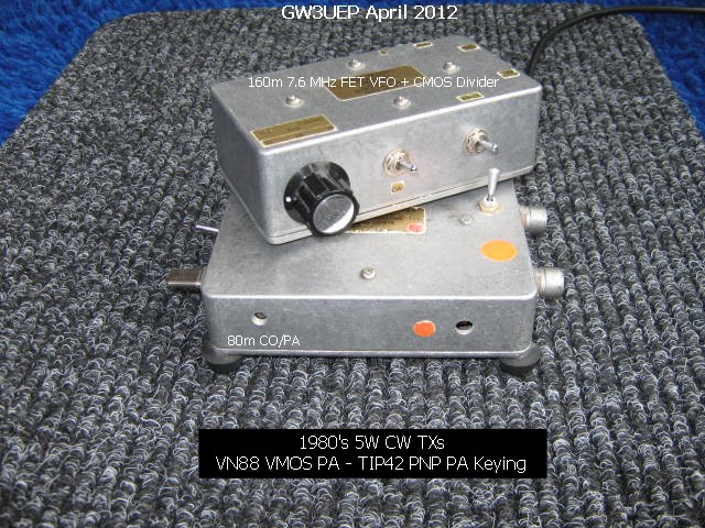
The 100W
MF CW transmitter and 25W QTX [Quick-TX] were developed from earlier
VMOS
Versions used on 160/80m/70MHz in the 1980’s. Higher power versions
followed on 160m [IRF630 50W & THX15 100W] and
80/60m
[IRF510 25W] with the simple current-boost circuit providing the required
gate-charge current. All versions used the same L-section output
configuration with high efficiency. When the 500kHz SRP/NOV arrived in 2007, the
solution was to hand and the QTX was born! Thanks to GW4HXO and EI0CF for their collaboration in construction,
evaluation and on-air-testing of the transmitters.
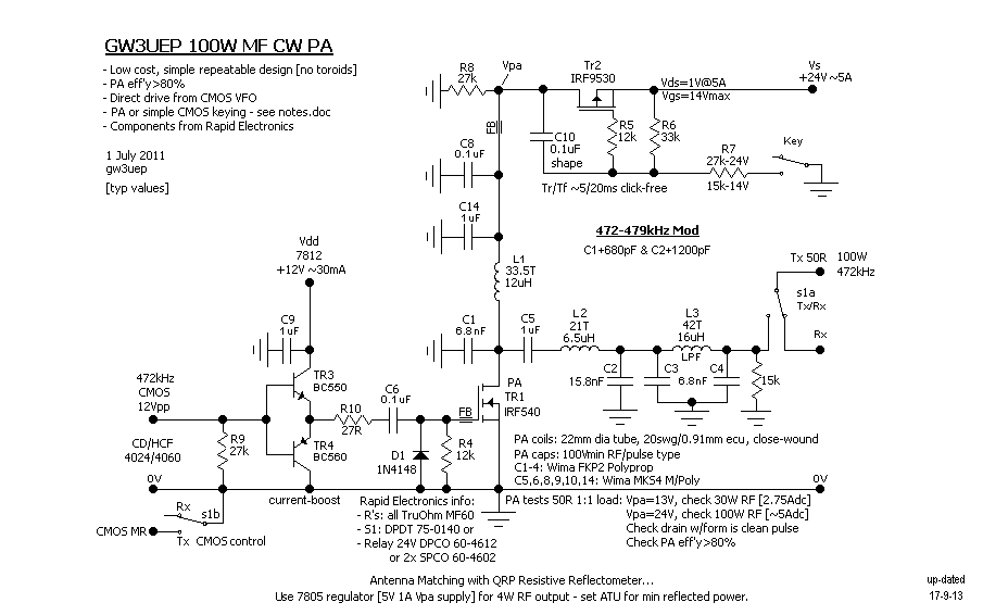
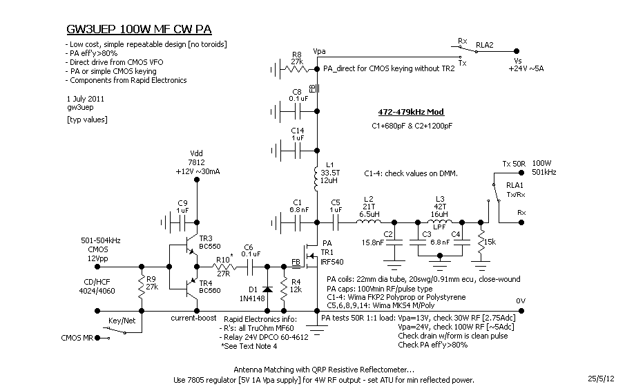
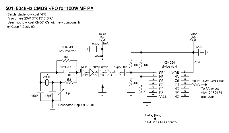
VFO circuit
CMOS 4049 Hex-Inverter
[IC1] with 2MHz ceramic-resonator provides a temperature stable VFO. The buffered 5Vpp output is ac-coupled to 4024 divider [IC2], which delivers 12Vpp output at 501-504 kHz. Frequency stability is optimised by low power
/ continuous operation of the oscillator circuit. The VFO box is separate from the PA unit in
order to avoid thermal coupling and temperature change.
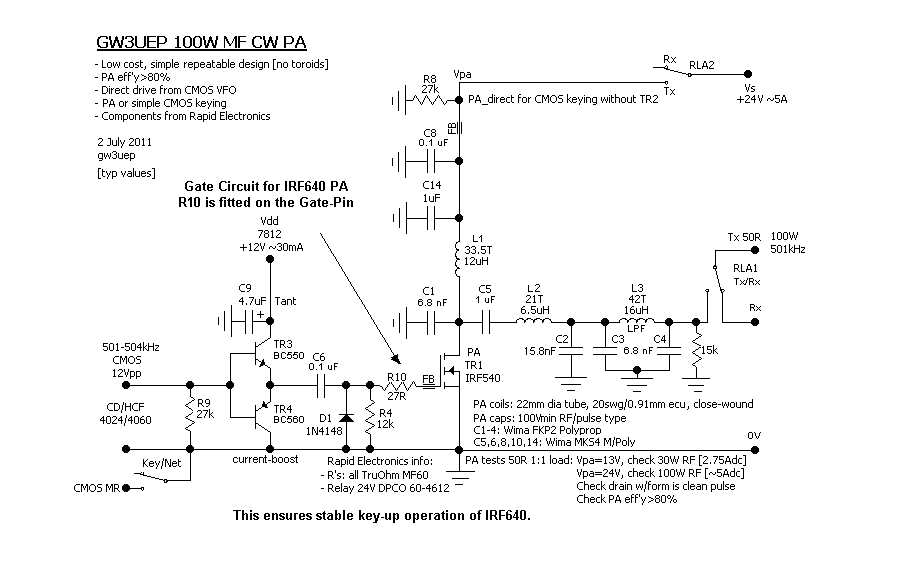
PA circuit
The IRF540 [TR1] was chosen
for operation at 500kHz for its low-cost rugged-design
and low R_DS[on]. TR3/4 form a
zero-biased complementary voltage-follower, buffering IC2 output-stage and
providing adequate source/sink current for the IRF540 gate-charge. The gate is ac-coupled and dc-restored to
ground should a dc-drive fault occur.
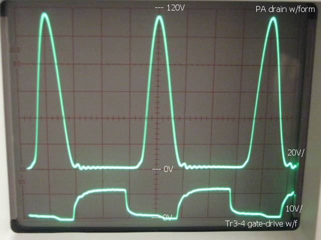
The PA operates in Class-D with drain efficiency in the 80%
range. The output circuit provides
matching and LPF functions, presenting a clean sine-wave to the 50R load. C1/L1 form a resonant MF tank-circuit. L-section C2/L2 transforms
the 50R load into the drain circuit load and is optimised for maximum
efficiency.
PA keying is achieved with
P-FET TR2, which also shapes the keyed RF envelope and eliminates key-clicks.
R6/R7 switch TR2 and along
with C10 set the rise and fall times. R5
ensures stability by rolling-off the frequency response of TR2, forming a LPF
with its input capacitance. TR2 drops 1V
at 5A / 100W RF output.
Simple
CMOS keying is
achieved using the VFO divider 4024 reset-line.
TR2 is replaced by RLA2 contacts, which remove the PA drain supply
on receive for key-down netting. The
keyed RF envelope is free from spikes and glitches, minimising local
key-clicks.
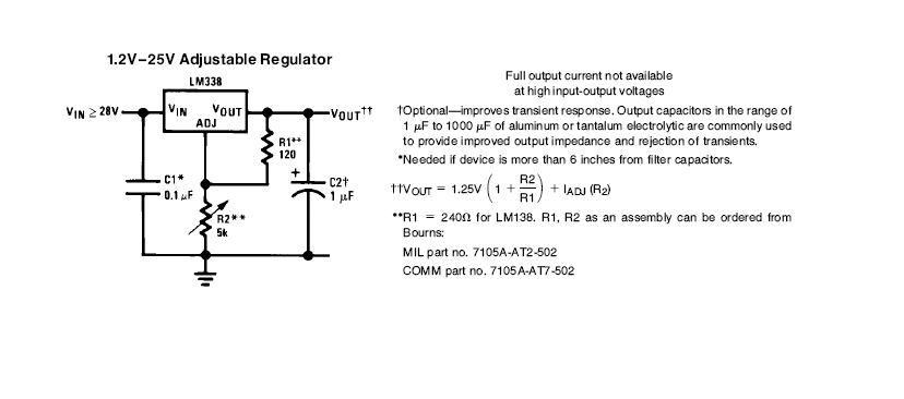
PSU
Regulated 24V PSU with current limiting set to ~5A. The LM338T provides a simple low-cost solution - Schematic
Operation over the range 14-25V is recommended. For QRP antenna matching see note on Schematic & QRP Meter
Setting-up [Typical values at 24V dc using DVM & Scope/10:1 probe for RF tests]
Terminate
VFO: check RF & dc values are as shown on VFO Schematic
PA: check <2mA dc TX/RX [no CMOS input, excludes relay & regulator current].
With CMOS input: check >10Vpp 501 kHz across R4 [Vpa= 0V].
TX key-down: check 100W RF output / 5A dc [30W RF / 3A dc with 14V supply].
Check PA Drain Waveform is a clean pulse as per scope shot and that efficiency is >80%.
Notes:
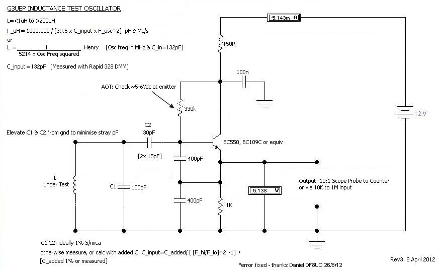
1] L1-3 values measured with
simple test-oscillator – see schematic
InductanceTestOsc
2] TR3/4
alternatives: BC549/559, BC337/327,
or BC109/BCY71, 2N3904/3906.
3]
Antenna system: ensure that a matched-load of <1.25:1 is presented to the TX.
4] TR1: if other devices are used [e.g. IRF640], fit R10 directly on the PA Gate-pin
5] For simple RF test circuits see MF Test Gear & QRP Meter
6] For 25W versions - see 25W QTX or 472 PA
7] 472kHz operation - see 100W Schematic
GW3UEP Index - updated 15/11/15